
New project: Japan's semiconductor revitalization and protection
update on a year-long assessment supported by Berkeley Risk & Security Lab

Friends,
This will be a bit of a build.
a) Back in November 2023, we had the pleasure of hosting the then-minister of METI, Nishimura Yasutoshi, for a special fireside interview at the Haas School of Business, followed by the signing of an MOU between JETRO (under METI), and Berkeley SkyDeck.

In Q&A (with questions from
) Minister Nishimura1 provided impassioned (and all the more impressive for being off the cuff) remarks about the Rapidus initiative in Chitose, Hokkaido. (We unpacked this in Clusters class the following week - conveniently, in a class on national technology strategies.)b) In December 2023, I joined the Circuit podcast to discuss this, and the topic of semiconductors in Japan more generally.
Appearance on the Circuit podcast: Japan's semiconductor industry

tune into the Circuit Podcast, episode 45, for more
c) Also in fall 2023: I joined the advisory board of the Berkeley Risk and Security Lab, which: seeks to bring robust academic research at the intersection of technology and security into policy spaces worldwide, while providing a common resource for learning, exploration, and engagement to the UC Berkeley campus, broader academic community, and public and private sectors.
A word about the formation of BRSL from faculty director Andrew Reddie here.
d) In June 2024, I wrote about a talk I gave in Tokyo in May, on the significance of where semiconductor fabrication happens.
If you build it, will they come? (Part 1)

Of warm starts and cold starts, and the employment multiplier
Which all gets us to the subject of this post.
In November 2024, BRSL lab director Leah Walker and I hosted representatives of the Consulate of Japan in San Francisco and METI and JETRO on campus for a briefing on a new project assessing Japan’s semiconductor revitalization and protection (protection in the economic security sense).
Why economic security? In May 2022, the Japanese government had passed its Economic Security Promotion Act, which laid out four priority tracks for legislative solutions:
the “system for ensuring stable supply of critical products,”
the “system for ensuring stable provision of essential infrastructure services,”
the “system for enhancing development of specified critical technologies,” and
the “system for non-disclosure of selected patent applications.
So whereas the US CHIPS Act was, as the acronym states, about Creating Helpful Incentives to induce Production of Semiconductors in the United States, Japan’s ESPA had an explicit economic security framing.
We explained that we would follow a clustering perspective in assessing the various areas where the governments Japan is investing in the revitalization of its semiconductor industry. Such areas include Kumamoto, Kyushu; Hiroshima; Tohoku; and Chitose, Hokkaido.
Investments are taking multiple forms, from subsidies going to existing producers, such as TSMC or Micron or Kioxia; to creation of new firms (e.g. Rapidus); to supplemental budgets for investment in infrastructure, such as that for water or wastewater treatment, or road capacity. Investments are also being made into human capital development, such as augmenting the semiconductor curricula at local universities.
Almost seven months later, I’m finally able to talk a little about this still-in-progress project. 😅
So far, I’ve made two trips to Japan for the purpose of stakeholder interviews.
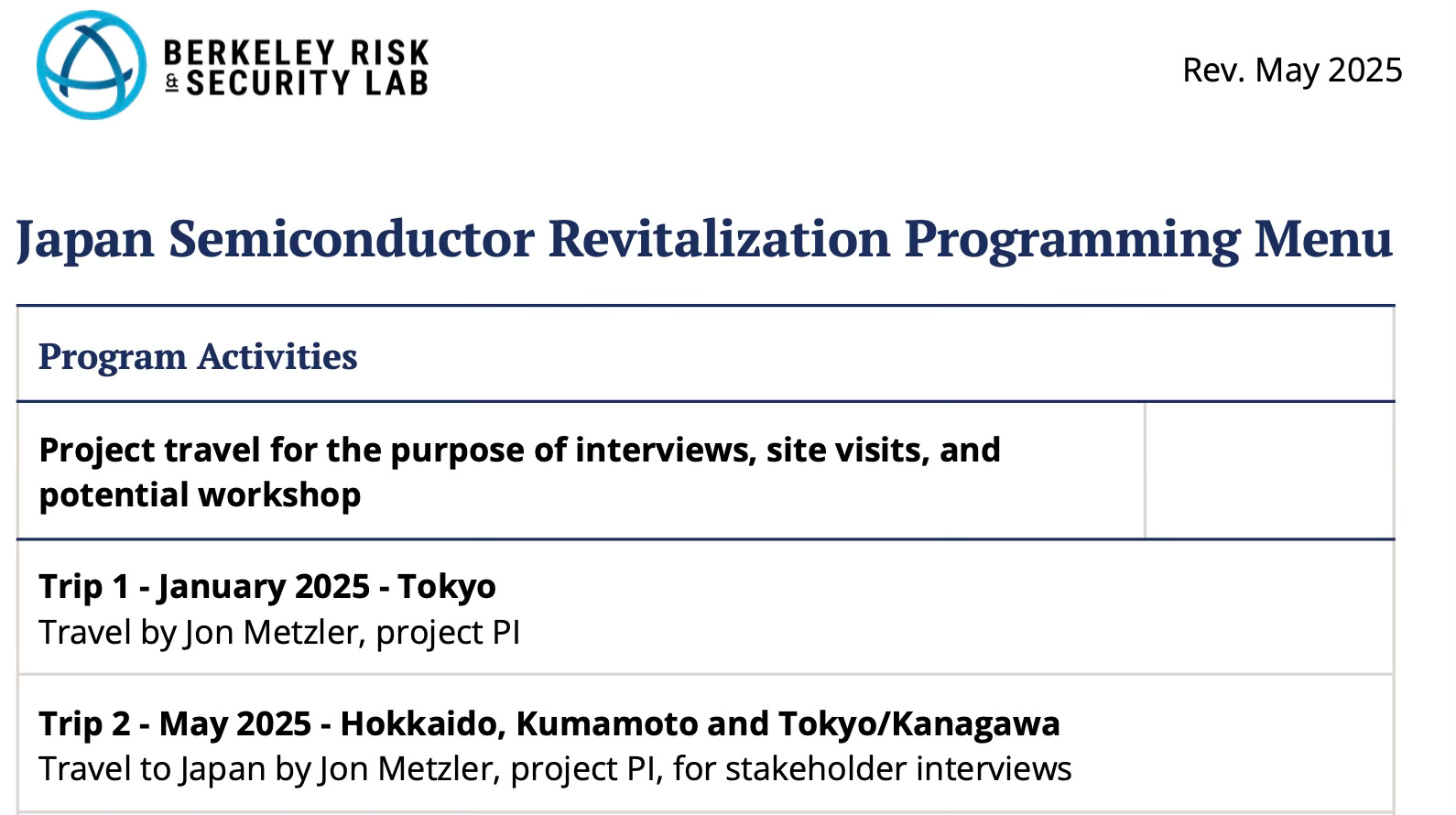
January 2025: mainly to meet with central government stakeholders as well as industry and academic stakeholders
May/June 2025: I visited Kumamoto, Kyushu, and Sapporo and Chitose in Hokkaido, before circling back to Tokyo and Kanagawa prefecture.
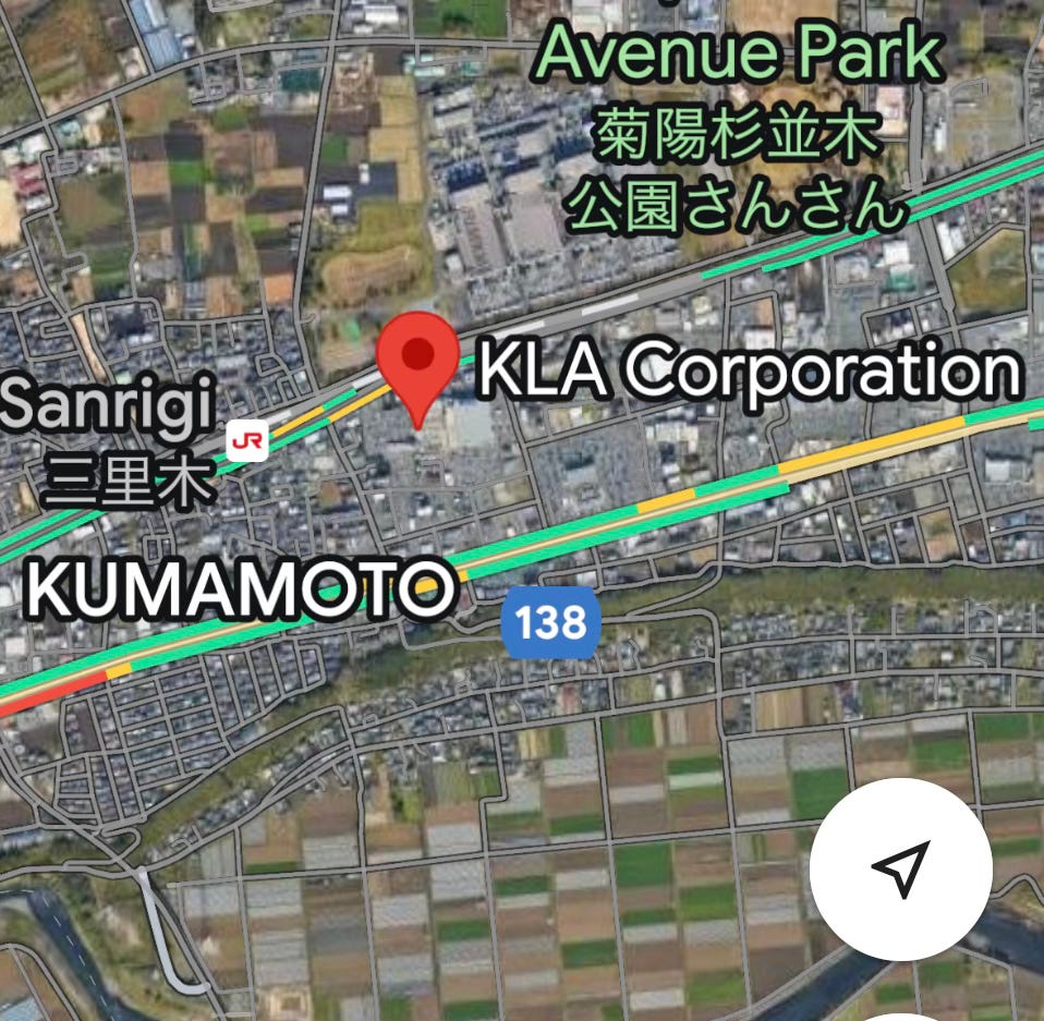
Kumamoto, Kyushu: the site of TSMC’s recently opened JASM fab , and also home to firms such as Tokyo Electron (TEL), Sony Semiconductor, and Renesas. ASML and KLA also have offices in the area. Kumamoto itself is one part of what Kyushu itself calls Kyushu: Silicon Island.
Kumamoto University graciously hosted me for meetings with faculty and administrators, and also help set up meetings with city and prefectural government. Many thanks to my gracious hosts, and to JETRO San Francisco and Professor Miyake Masato at Ritsumeikan University for their help and perspective.
I also visited the JASM operation and visited the local JETRO Kumamoto office. (Yes, fabs beggar description when you actually see them up close. They really are that big.)
More to come in subsequent posts and publications on these various conversations.
I will note that Kumamoto was an entirely logical place to put the first JASM fab, for many reasons, from nuclear power availability (Kyushu has two reactors operating) to abundant water (notably, groundwater - talk to anyone in Kumamoto at length and groundwater will come up, for natural and historic reasons) to industry presence and proximity (e.g. Sony and TEL) to site availability to collaborative local educational institutions, such as Kumamoto University and of course Kyushu University in Fukuoka.
One pleasant Kumamoto surprise but perhaps indicative of the town’s recent growth - seeing the local KLA and ASML offices as I passed a suburban shopping mall, next door to a local branch of the Yamada Denki electronics chain.
Following Kumamoto, I visited Sapporo and Chitose in Hokkaido, Japan’s northernmost prefecture. Chitose is home to the in-progress Rapidus IIM fab. Sapporo is home to Hokkaido University, one of the national universities and winner of two Nobel prizes. (The sports- or ski-minded will remember: in 1972, Sapporo hosted the Winter Olympics. I worked at the next Winter Olympics held in Japan, in Nagano in 1998. Here’s a past post on that. )
During my time in Hokkaido, Hokkaido University graciously hosted me for meetings with faculty, administrators, and the university startup accelerator, and also help set up meetings with city and prefectural (道庁) government stakeholders.
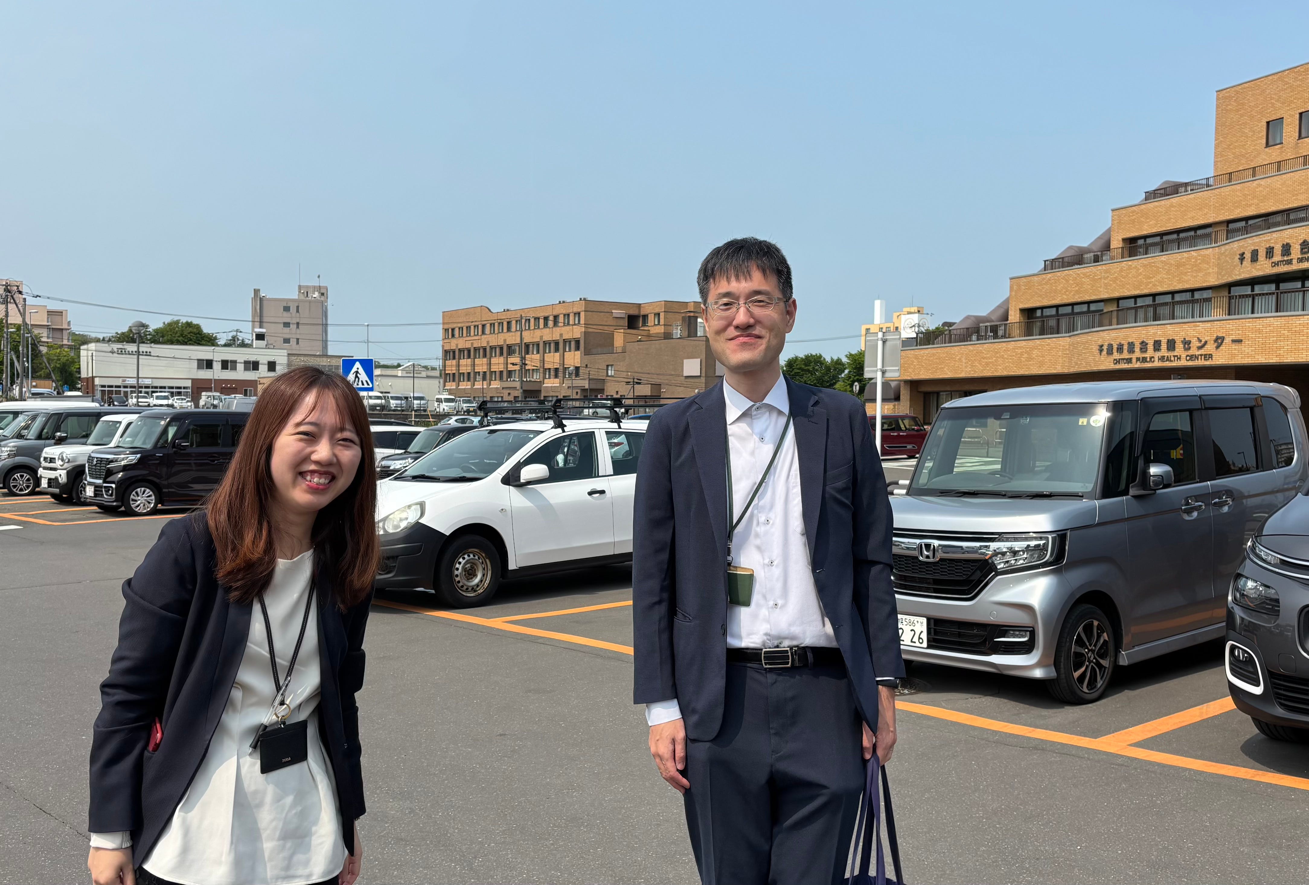
My gracious hosts from Hokkaido University’s semiconductor ecosystem promotion office
I also and visited the local JETRO Hokkaido office, and ANIC (Agency for the New Industry Cluster of Hokkaido), a local non-profit helping facilitate Hokkaido’s nascent but growing semiconductor ecosystem. (What about the Rapidus IIM fab, you ask? It’s still being built out. I saw many buses coming and going, full of construction workers. At its peak, contractor Kajima had some 3000 workers were on the project. Thus, I visited Rapidus in Tokyo.)
A particularly memorable highlight - a rich discussion with Hokkaido University faculty and administrators on the semiconductor ecosystem and research security, along with visiting scholar Ota Yasuhiko, long-term correspondent for Nikkei and author of 半導体の地政学 (The Geopolitics of Semiconductors).
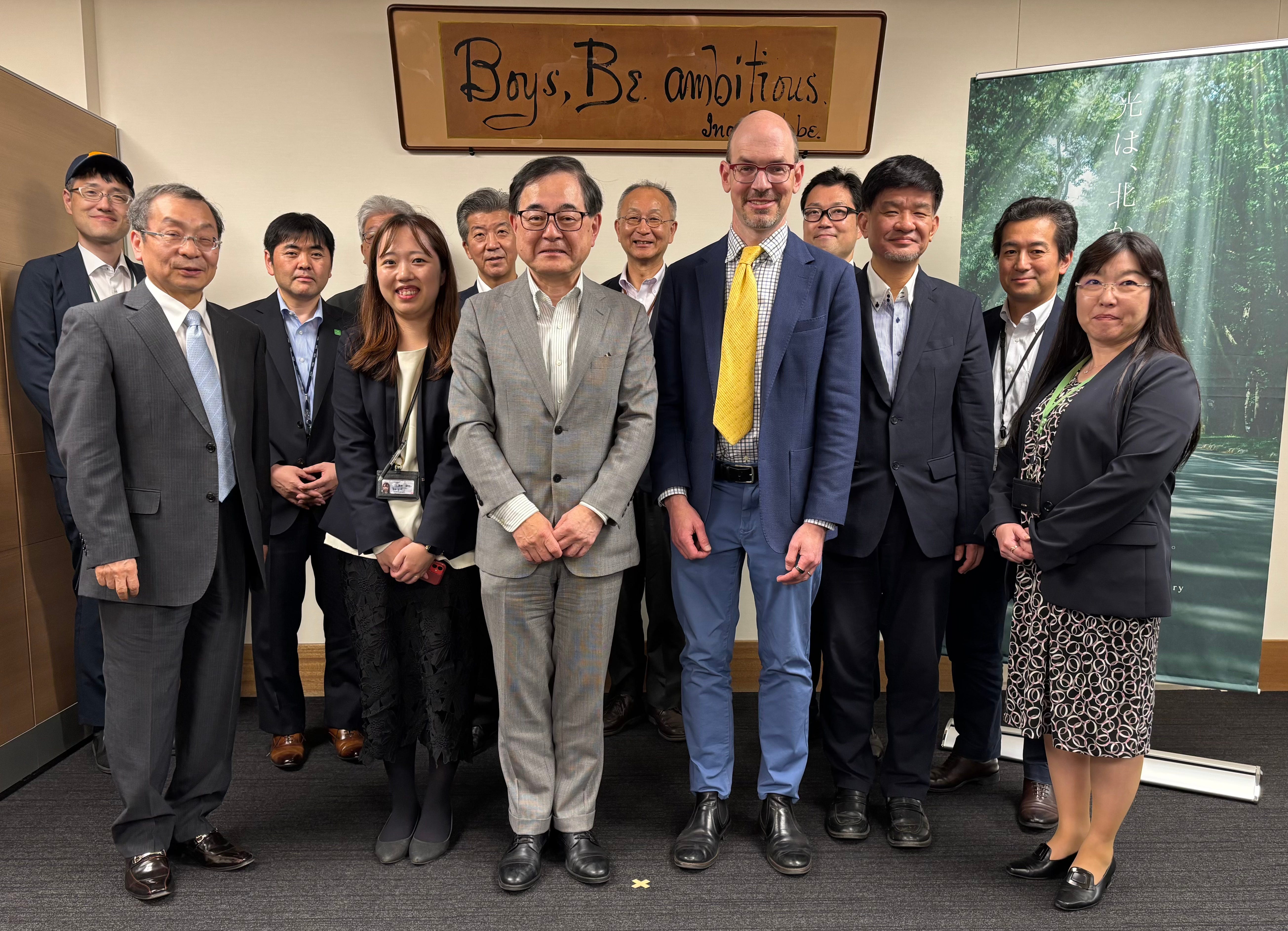
Hokkaido University president Houkin Kiyohiro, faculty and administrators, and members of the semiconductor ecosystem promotion office. (Bonus: can you find the Cal hat?)
There have been two significant discoveries already:
Increased interest in technology for security purposes, and how to build an ecosystem around that that is inspired by that in the US and the UK
Silicon photonics, or as NTT calls it “Photonics Electronics convergence” (光電融合). This was a topic of discussion pretty much everywhere I went - indeed, people asked if it was as much a topic in the States.
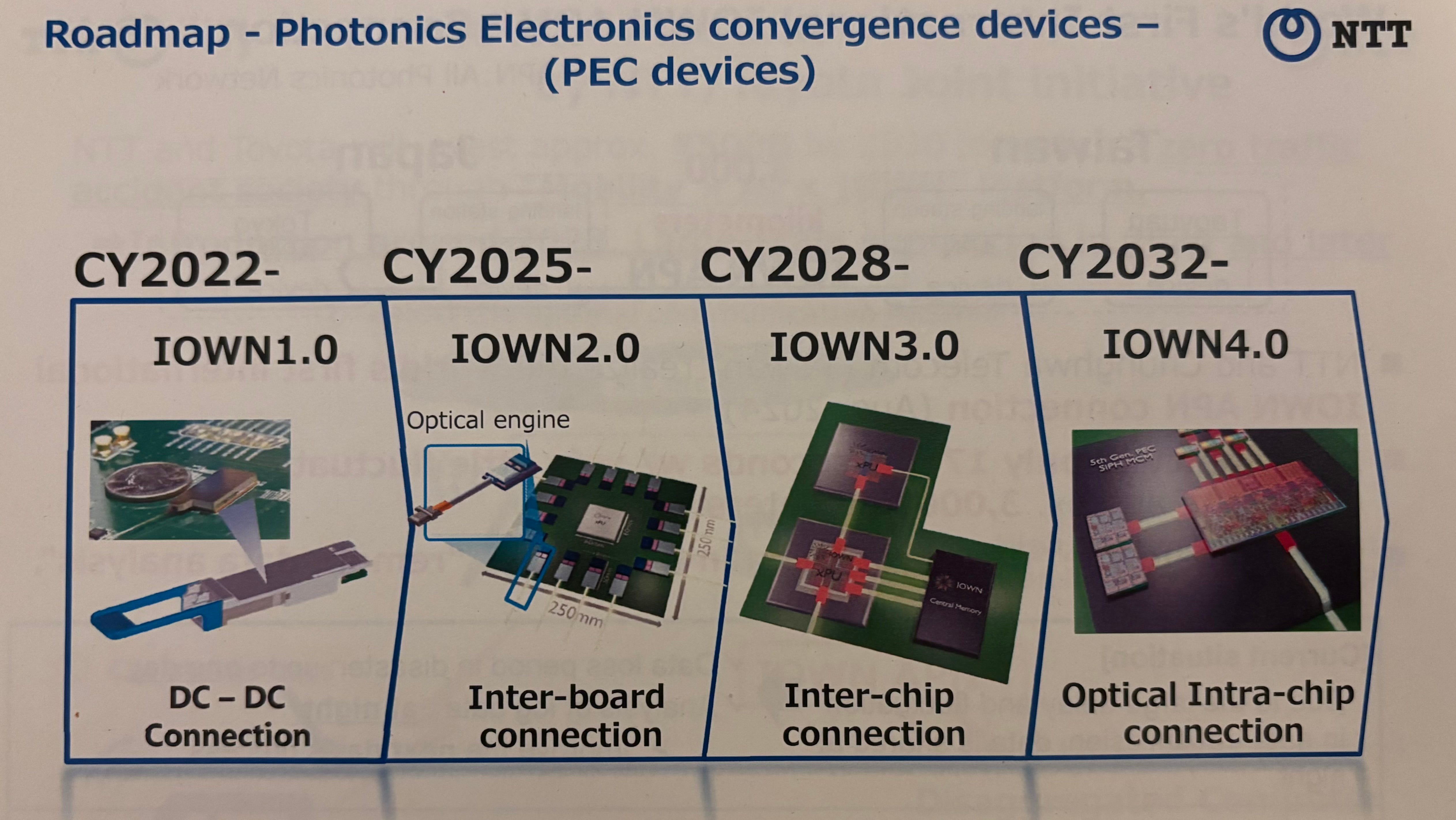
NTT IOWN roadmap
A LOT of people - in government, academia, and industry (産学官、the three strands of the triple helix, plus the fourth strand or the community strand) - have been very generous with their time and insights so far.
With that said, there’s a lot of work yet to do on the project. In particular, I will spend more time on the demand side (buyers of silicon, and also demand for fab capacity). Also, there are other areas of Japan to visit - in particular, Tohoku.2
With all those caveats, I am happy to announce that I will share observations from the work so far (on Rapidus’ positioning; on Japan’s nascent fabless sector; the two discoveries above and more) in an interview hosted by
in an upcoming episode of the Circuit podcast.Thanks to Jay for bringing me back for my second appearance. 🙏
Onward and upward! And more to come.
Jon
former Minister Nishimura is still a parliamentarian (Hyogo 9th district), and in May 2025 in Taipei, remarked on an “Iron Triangle” forming between Japan, Taiwan, and the United States
I should be in Japan in December, for Semicon Japan.
Delighted to make a return appearance on The Circuit podcast, hosted by @Digits to Dollars to discuss Japan’s semiconductor revitalization. Thanks, Jay, for having me back.
https://share.transistor.fm/s/f4a54990
Topics: visits to Kumamoto, Kyushu, and Sapporo and Chitose in Hokkaido; semiconductor education in Japan versus the US; and the Rapidus foundry initiative (which I characterize as the “Flex of logic”); TSMC’s first Japan fab
Shout-outs given to @Doug O'Laughlin and @Jon Y